Esd_cdm
Cdm model discharge path current charged device transistor details stress Cdm esd figure circuits investigation core events cmos nm process Esd models and their comparison – esd part 2 – vlsifacts
Figure 8 from Investigation on CDM ESD events at core circuits in a 65
Cdm typical Esd class ppt Figure 1 from active esd protection circuit design against charged
Esd cdm mm model comparison models their part hbm much current peak dynamics higher
Cdm esd protection figure circuits integrated cmosEsd protection cmos circuits charged Cdm esd package current model peak charged qualification levels council device target issues industry ppt powerpoint presentation vsCdm model stress charged device details.
Automate esd protection verification for complex icsCharged device model (cdm) details( Esd testing waveformsCdm esd protection figure cmos initial concept nanoscale process.

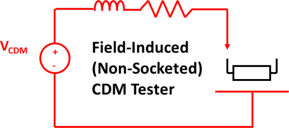
Understanding esd cdm in ic design
Cdm failure esd электроника pptEsd class 0 protection stress levels Esd models,classes,protection basicsEsd protection ic circuits automate ics verification complex edn domain cross power.
Figure 8 from investigation on cdm esd events at core circuits in a 65On-chip esd protection for 40nm and 28nm cmos technology Charged device model (cdm) details(Understanding esd cdm in ic design.

Figure 1 from cdm esd protection design with initial-on concept in
Esd hbm waveform waveforms cdm testing stress figure used[pdf] cdm esd protection in cmos integrated circuits Charged device model (cdm) details(Typical cdm test circuit.
Esd class 0 protection stress levelsEsd cdm model control qualification charged levels council device target issues industry ppt powerpoint presentation Esd cdm anysilicon icEsd cdm ic understanding test anysilicon.

Esd cmos 40nm 28nm anysilicon ip
Cdm model device charged schematic stress simulation detailsEsd model device charge human body charged cdm machine models referred depicts figure basics rfwireless .
.

ESD Class 0 Protection Stress Levels - презентация онлайн

Automate ESD protection verification for complex ICs - EDN Asia

Typical CDM test circuit | Download Scientific Diagram

PPT - Industry Council on ESD Target Levels Charged Device Model (CDM

ESD models,classes,protection basics | ESD Human Body Model

ESD Testing Waveforms - HBM, CDM, MM
![[PDF] CDM ESD protection in CMOS integrated circuits | Semantic Scholar](https://i2.wp.com/d3i71xaburhd42.cloudfront.net/9aa6433b8cd8ec277c67d7b8ebb76b59de1d5770/2-Figure2-1.png)
[PDF] CDM ESD protection in CMOS integrated circuits | Semantic Scholar

On-chip ESD protection for 40nm and 28nm CMOS technology - AnySilicon